FE-SEM + EDS
Field-emission SEM (Scanning Electron Microscope)
Thermo Scientific Apreo S
with
Oxford Instruments UltimMax 100 Energy Dispersive X-ray Spectrometer (EDS)
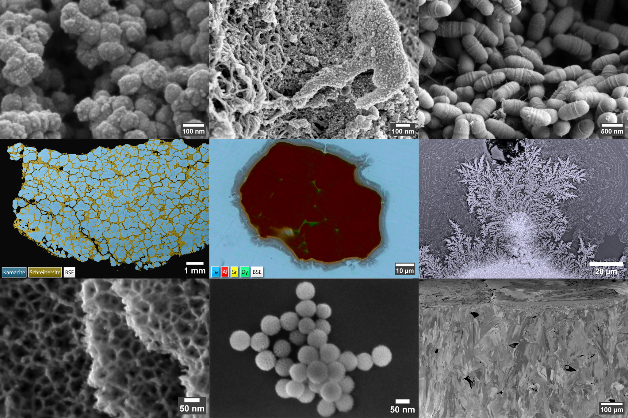
This field-emission SEM can be used for high-resolution imaging and to obtain compositional and elemental information of the surface or near-surface region of different samples.
SEM is useful for materials science and for industrial manufacturing and can be used to image materials ranging e.g. from nano- and microparticles, catalysts, and nanodevices to bulk magnetic samples and insulators such as polymers. SEM can also be used in biological sciences for imaging e.g. fixed cells or tissue blocks at high magnifications. Our FE-SEM has also broad analytical extensions, such as STEM (Scanning Transmission Electron Microscopy) detector for TEM grid imaging, Cathodoluminescence detector (CLD) and EDS detector for elemental analysis.
For more information, contact Ermei Mäkilä.
Specifications:
- Acceleration voltages from 0.2 kV to 30 kV
- Multiple in-lens and in-column detectors for high resolution, low voltage SE and BSE imaging
- Segmented retractable BSE and STEM detectors and RGB + Panchromatic CL detector
- 5-axes motorized sample stage, with 110 x 110 mm XY motion, full rotation and -15° to +90° tilt
- Maximum sample weight 500g with tilt
- Low vacuum SE/BSE imaging up to 500 Pa
- Stage biasing (beam deceleration) from +600 V to -4000 V
- Multiple final lens modes: Field-free analytical mode, electrostatic final lens (for e.g. magnetic materials) and compound immersion magnetic lens (for non-magnetic samples)
- AZtec 6.1 software for EDS control, including large area mapping and particle size and feature analysis.
- Local installation of AZtec 6.3 for off-site data analysis possible and recommended for UTU users
For more information, contact Ermei Mäkilä.
Note to academic users:
Note that all academic users are required to acknowledge the use of the infrastructure in all publications such as journal articles and theses, where the data obtained is published:
We acknowledge the Materials Research Infrastructure (MARI) at Department of Physics and Astronomy, University of Turku for access and support with the SEM facilities.